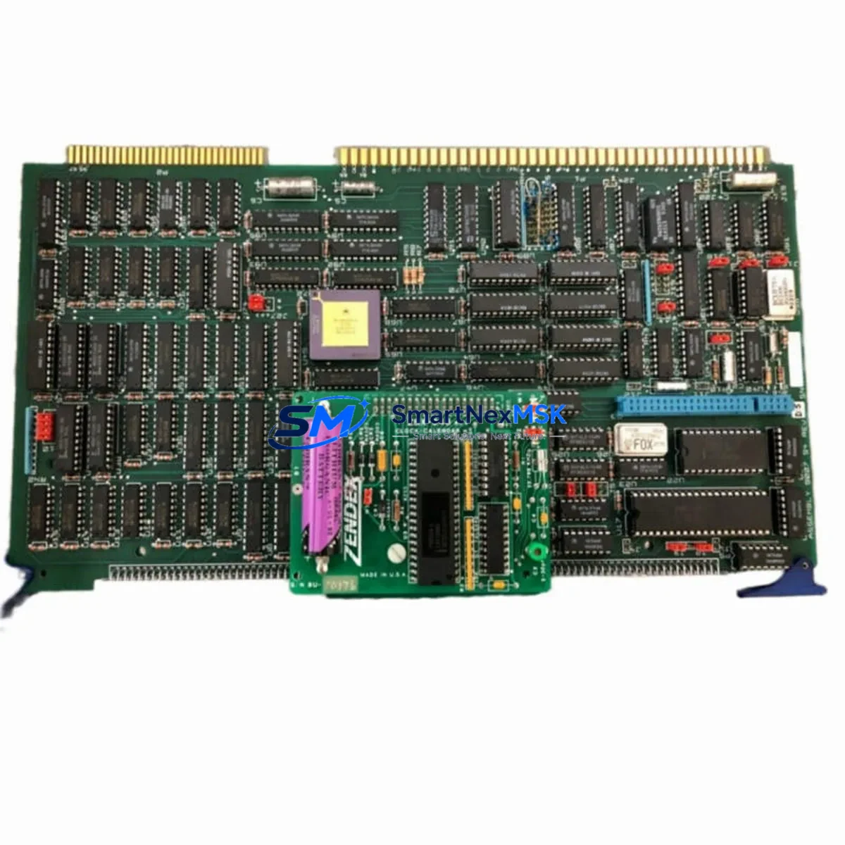
SBE M68CPU Retrofit-Ready CPU Module for MULTIBUS I Control Systems
The SBE M68CPU is a Motorola 68000-based central processing unit card engineered for seamless integration into MULTIBUS I (IEEE 796) backplane architectures. As legacy control systems across manufacturing, utilities, and process industries reach end-of-life, the M68CPU has become a critical retrofit component for engineers tasked with extending the operational lifespan of existing automation infrastructure without a full platform migration.
Whether you are replacing a failed CPU card in a running production line, upgrading processing capacity in an aging control cabinet, or restoring a system after an unplanned shutdown, the SBE M68CPU delivers the electrical and mechanical compatibility required for a reliable, low-risk retrofit. SMARTNEXMSK maintains verified stock of this module with full pre-shipment functional testing and a 12-month warranty on every unit.
Upgrade Compatibility Table
| Parameter | SBE M68CPU Specification | Retrofit Notes |
|---|---|---|
| Bus Architecture | MULTIBUS I / IEEE 796 | Direct backplane compatibility; verify slot pitch and card guide clearance |
| Processor | Motorola MC68000 (8/10 MHz) | Confirm clock speed matches existing system timing requirements |
| Bus Width | 16-bit data / 24-bit address | Compatible with standard MULTIBUS I memory and I/O cards |
| Power Requirements | +5 VDC, +12 VDC, −12 VDC | Verify backplane PSU capacity before installation; check SBE power supply modules |
| Terminal / Connector | P1 + P2 edge connectors (IEEE 796) | Inspect connector pins for oxidation; clean with contact cleaner before seating |
| Communication | Serial (RS-232/RS-422 via UART) | Confirm baud rate and protocol settings match existing HMI and SCADA links |
| Memory Interface | Compatible with MULTIBUS I EPROM/RAM cards | Re-seat or replace SBE memory modules if checksum errors occur post-swap |
| Installation | Single-slot, standard MULTIBUS I card format | No mechanical modification required for standard chassis |
| Replacement Scope | Direct drop-in for failed or obsolete M68CPU units | Retain original DIP switch and jumper settings from removed card |
| Warranty | 12 Months | Covers manufacturing defects; includes pre-shipment functional burn-in test |
Retrofit Planning for Existing Automation Systems
A successful M68CPU retrofit begins well before the card is physically installed. Engineers should start by auditing the full MULTIBUS I chassis to document every occupied slot. In a typical legacy control cabinet, the M68CPU shares the backplane with SBE memory expansion cards (EPROM and static RAM modules), MULTIBUS I parallel I/O boards for discrete input/output, and analog I/O modules handling 4–20 mA process signals. Each of these cards must be confirmed operational before the CPU swap, as a pre-existing fault on a peripheral card can be misdiagnosed as a CPU failure.
Power budget verification is non-negotiable. The MULTIBUS I backplane distributes +5 VDC, +12 VDC, and −12 VDC rails, and the SBE power supply module feeding the chassis must have sufficient headroom to support the M68CPU alongside all co-resident cards. Measure actual rail voltages under load before and after the swap. If rail voltages sag below tolerance, the power supply module itself may require replacement or supplementation.
For systems that include a MULTIBUS I serial communication card or a dedicated RS-232/RS-422 interface module, the communication parameters — baud rate, parity, stop bits, and station address — must be documented from the original configuration. These settings govern the link between the CPU and any connected operator interface terminals (OIT) or upstream SCADA systems. After the M68CPU is seated, re-establish each serial link individually and confirm data integrity before returning the system to automatic mode.
If the control system includes a MULTIBUS I DMA controller card or a bus arbitration module, verify that the new M68CPU’s bus request and grant timing is compatible. Some early MULTIBUS I arbiters have fixed priority schemes that may require jumper adjustment when a CPU card is changed. Similarly, if a MULTIBUS I watchdog timer card is present, confirm that the M68CPU’s heartbeat output meets the timer’s pulse width requirements to prevent nuisance resets during commissioning.
Program memory is typically held in EPROM devices mounted on a dedicated SBE EPROM memory card or socketed directly on the CPU card itself. Before removing the original M68CPU, photograph or document all EPROM part numbers and socket positions. If the application program is stored on the CPU card’s on-board EPROM sockets, the EPROM devices must be transferred to the replacement card with the same socket mapping. Verify the program checksum using the system’s built-in diagnostic routine or a standalone EPROM programmer before powering up.
HMI screen layouts and tag mappings tied to specific memory addresses should be reviewed against the replacement CPU’s memory map. In systems where a MULTIBUS I graphics or text display controller card drives the operator interface, address conflicts can cause display anomalies that are easily resolved by adjusting the display card’s base address jumpers.
Downtime Control During System Migration
Minimizing unplanned downtime during a MULTIBUS I CPU replacement requires a structured pre-outage preparation protocol. Begin by creating a full backup of all EPROM program images using a compatible programmer. If the system uses battery-backed SRAM for data retention, note the battery condition and replace it proactively — a failed backup battery on a MULTIBUS I SRAM card will cause data loss the moment power is removed.
Schedule the physical swap during a planned maintenance window. Have the replacement M68CPU, a set of known-good MULTIBUS I peripheral cards, and all required tools staged at the control cabinet before the system is powered down. The actual card exchange — removing the original CPU, transferring EPROM devices if required, setting DIP switches and jumpers to match the original configuration, and seating the new card — typically takes 15 to 30 minutes for an experienced technician.
After power-up, follow a structured commissioning sequence: confirm power rail voltages, verify the CPU’s diagnostic LED sequence, check serial communication links to the HMI and SCADA, exercise discrete I/O points through the operator interface, and run a controlled process cycle before releasing the system to production. Keeping a commissioning checklist specific to the M68CPU retrofit ensures no step is skipped under time pressure, protecting both the equipment and the original program logic.
SMARTNEXMSK ships all M68CPU units with a pre-shipment functional test report. Units are burned in under load to screen for early-life failures before dispatch, reducing the risk of a repeat outage caused by an infant-mortality failure in the replacement card.
Retrofit Support FAQ
Q1: Is the SBE M68CPU a direct drop-in replacement for my existing MULTIBUS I CPU card?
In most cases, yes. The M68CPU conforms to the IEEE 796 MULTIBUS I mechanical and electrical standard, making it physically and electrically compatible with any standard MULTIBUS I chassis. You must replicate the original card’s DIP switch and jumper settings — particularly clock speed selection, memory address decoding, and interrupt level assignments — before powering up. SMARTNEXMSK provides configuration guidance based on your system documentation.
Q2: How do I verify wiring and terminal compatibility before installation?
The M68CPU connects exclusively through the P1 and P2 edge connectors defined by the IEEE 796 standard. No field wiring terminates directly on the CPU card; all I/O wiring connects to dedicated I/O modules on the backplane. Inspect the backplane connector for bent or corroded pins and clean with an appropriate contact cleaner. Verify that the chassis card guides are undamaged and that the replacement card seats fully without mechanical interference.
Q3: What commissioning steps are required after installing the replacement M68CPU?
After seating the card and restoring power, confirm the CPU’s self-test LED sequence completes without fault codes. Re-establish all serial communication links and verify data exchange with connected HMI terminals and SCADA systems. Exercise all I/O points through the operator interface and run a supervised process cycle. Document the commissioning results and retain the pre-shipment test report supplied with the unit for your maintenance records.
Q4: What does the 12-month warranty cover, and what is the return process?
The 12-month warranty covers manufacturing defects and functional failures under normal operating conditions. It does not cover damage caused by incorrect installation, overvoltage, or physical mishandling. If a warranty claim is required, contact SMARTNEXMSK with the unit serial number and pre-shipment test report. A replacement or repair will be arranged with priority handling to minimize your system downtime.
© 2026 SMARTNEXMSK. All rights reserved.
Original Source: https://smartnexmsk.com
Contact: sales@smartnexmsk.com | +86 18259474341