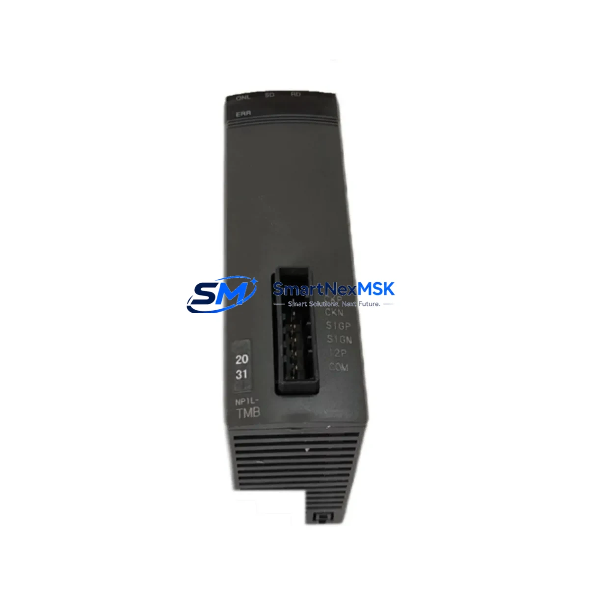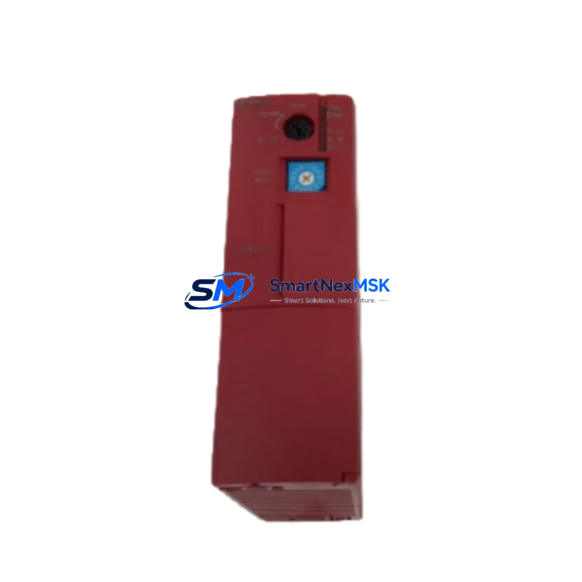
FUJI EP-3965A-C2 Retrofit-Ready Gate Drive Board for FUJI VFD Series Control Systems
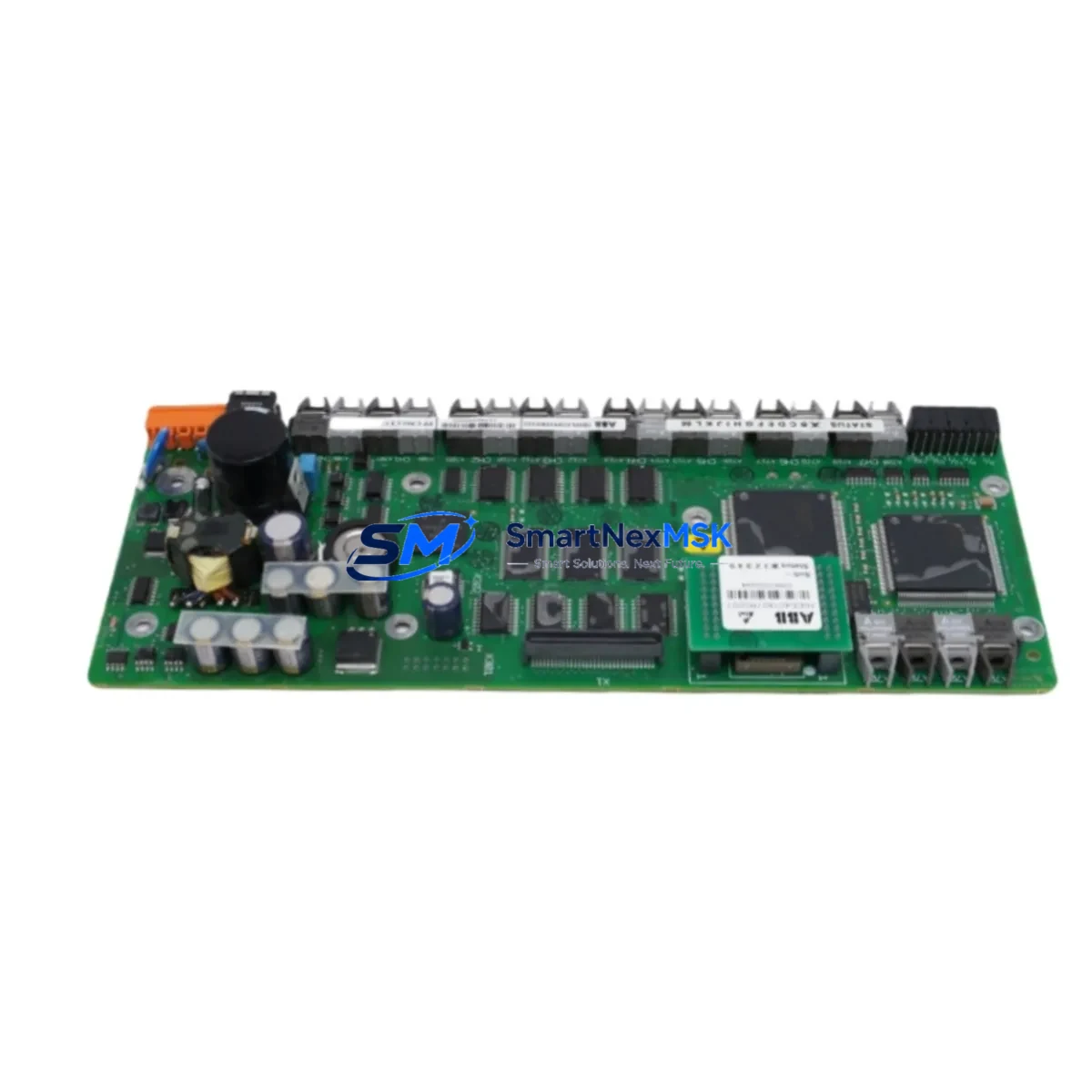
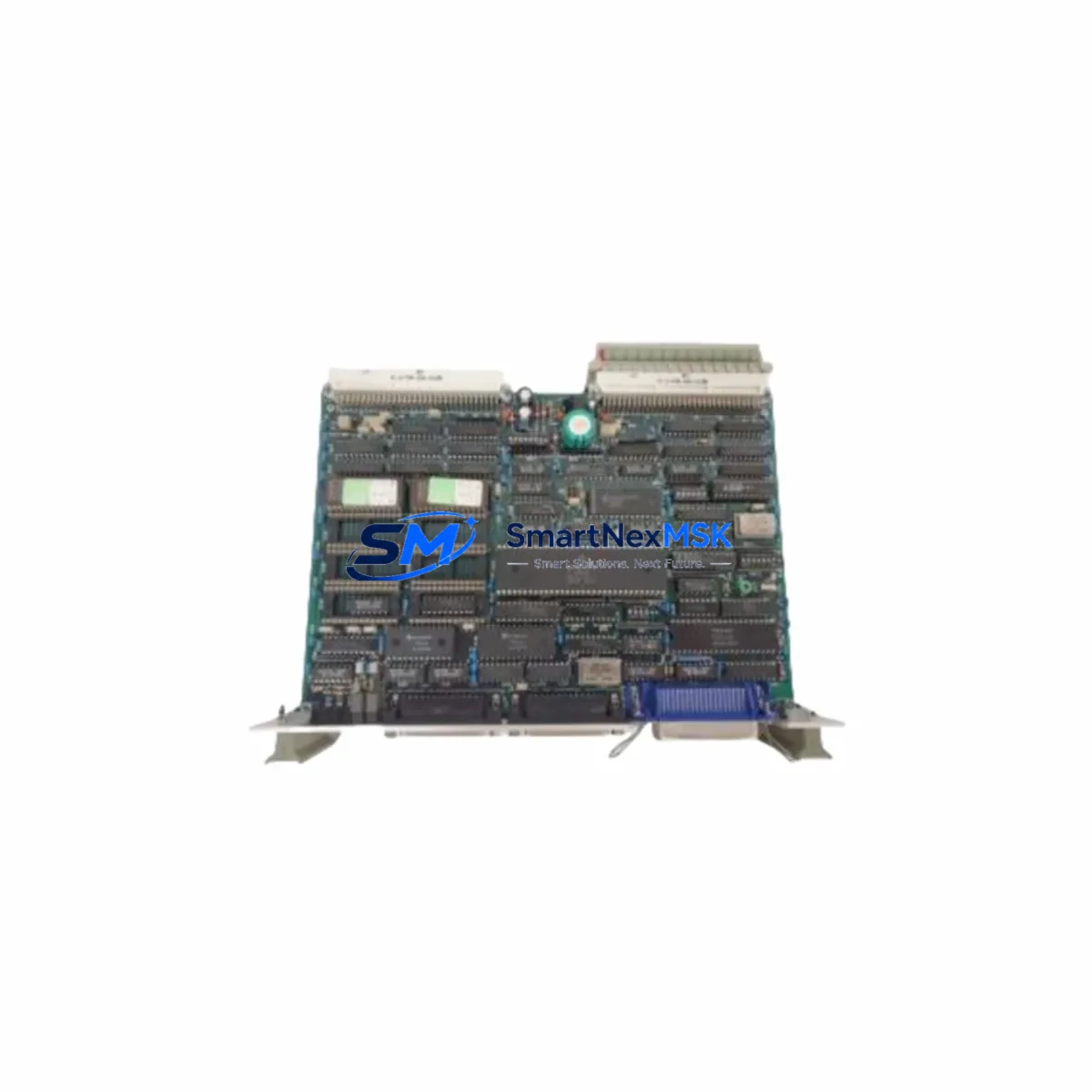
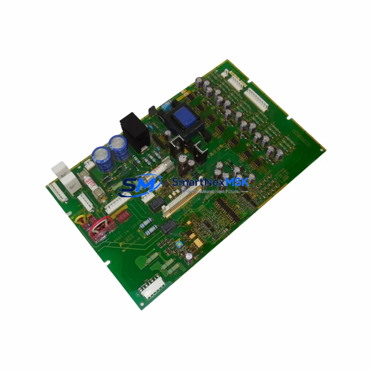
The FUJI EP-3965A-C2 is a gate drive printed circuit board engineered for FUJI Electric variable frequency drive (VFD) inverter systems. As legacy FUJI inverter platforms approach end-of-life and OEM spare parts become increasingly scarce, the EP-3965A-C2 serves as a verified retrofit-ready replacement that enables engineers to restore full drive functionality without replacing the entire inverter cabinet or control system. Whether you are recovering from an unplanned drive failure, executing a planned control system upgrade, or building a strategic spare-parts inventory for critical production lines, the EP-3965A-C2 delivers the electrical compatibility and mechanical fit required for a smooth, low-risk transition.
This board is designed to interface directly with the IGBT power module stack and main control board within the FUJI VFD inverter chassis. It handles gate signal conditioning, isolation, and fault feedback — functions that are central to safe and efficient motor speed regulation. When the original gate drive board fails due to overvoltage stress, thermal cycling fatigue, or component aging, replacing it with the EP-3965A-C2 restores the inverter to factory-equivalent performance without requiring firmware changes or drive reconfiguration in most standard applications.
Upgrade Compatibility Table
| Parameter | Details |
|---|---|
| Compatible Series | FUJI FRENIC Series VFD Inverters (FRENIC-Mini, FRENIC-Multi, FRENIC-Mega) |
| Board Function | IGBT Gate Drive, Isolation, Fault Feedback |
| Mounting Interface | Direct PCB slot / backplane connector — matches OEM mechanical footprint |
| Communication Compatibility | Compatible with existing FUJI inverter control board signal architecture |
| Terminal Wiring | Retain original wiring harness; verify connector polarity before insertion |
| Replacement Recommendation | Direct drop-in for failed or degraded OEM EP-3965A-C2 boards |
| Commissioning Notes | Verify IGBT module condition before installation; run no-load test after fitting |
| Warranty | 12-Month Warranty — covers manufacturing defects and functional failure under normal operating conditions |
Retrofit Planning for Existing Automation Systems
Successful retrofit of the EP-3965A-C2 into an existing FUJI VFD installation requires a structured approach that accounts for the full drive assembly and its integration with the broader automation system. Before removing the failed board, engineers should document the current inverter parameter settings using the FUJI keypad operator panel or a connected PC loader tool, as parameter data stored in the main control board — such as the FUJI OPC-G1-PG or OPC-G1-RY option cards — may need to be re-verified after the repair.
The gate drive board sits between the main control PCB and the IGBT power module. When planning the swap, confirm that the IGBT module itself — typically a dual or six-pack module rated to the inverter’s output current class — is not damaged. A shorted IGBT will destroy a new gate drive board immediately upon power-up. Use a multimeter or dedicated IGBT tester to verify module integrity before installing the EP-3965A-C2.
For inverters integrated into a PLC-controlled production line — for example, systems using a FUJI MICREX-SX series PLC or a third-party Siemens S7-300 controller communicating over PROFIBUS-DP or Modbus RTU — the drive replacement should be treated as a node substitution event. Confirm that the inverter station address, baud rate, and communication timeout parameters are correctly restored after the board swap. If the inverter communicates via a FUJI RS-485 option card or a DeviceNet adapter module, re-initialize the communication link and verify that the PLC program receives the expected drive status feedback before resuming automatic operation.
In control cabinets where the FUJI VFD shares a 24 VDC auxiliary power rail with other devices — such as terminal relay modules, I/O expansion blocks, or an HMI panel like the FUJI V9 series or a Proface GP4000 series touch panel — verify that the auxiliary power supply capacity is sufficient after the repair. A degraded gate drive board can sometimes cause abnormal current draw on the 24 VDC rail, and restoring the board to a healthy state may change the load profile. Check the power supply output voltage under full load before closing the cabinet.
If the retrofit is part of a broader control system modernization — for instance, migrating from an older FUJI FRENIC5000 G11 series drive to a current FRENIC-Mega platform — the EP-3965A-C2 may serve as an interim solution to keep the legacy drive operational while the new drive is being configured, wired, and commissioned in parallel. This staged approach minimizes production downtime and allows the engineering team to validate the new drive’s parameter set and I/O mapping against the existing PLC logic before the final cutover.
For multi-axis systems where several FUJI inverters share a common DC bus or are mounted in a common inverter rack with a shared braking resistor unit, isolate the affected drive from the DC bus before beginning the board replacement. Confirm that the braking resistor and its associated discharge circuit are functioning correctly, as a failed gate drive board can sometimes be caused by regenerative energy events that exceed the braking capacity of the system.
Downtime Control During System Migration
Minimizing unplanned downtime during a gate drive board replacement is a primary concern for any production environment. The EP-3965A-C2 is supplied from verified stock with pre-shipment functional testing, which eliminates the uncertainty associated with sourcing untested surplus components. Upon receipt, the board should be stored in its anti-static packaging until the maintenance window begins.
To protect the original program logic and control continuity, ensure that the PLC controlling the drive is placed in a safe hold state before the inverter is de-energized. For systems using a FUJI MICREX-SX or similar controller, activate the drive fault interlock in the PLC program to prevent automatic restart commands from being issued during the repair window. If the system uses a distributed I/O architecture — for example, FUJI FLEX-PC I/O modules or a remote I/O rack connected via CC-Link — verify that the I/O rack remains powered and communicating with the PLC throughout the repair to avoid cascading fault conditions in other parts of the line.
After installing the EP-3965A-C2, perform a no-load power-up test with the motor disconnected from the drive output terminals. Verify that the drive displays no fault codes and that the gate drive status indicators — where visible — show normal operation. Reconnect the motor and perform a low-speed jog test before returning the drive to automatic control. Document the repair in the equipment maintenance log, including the board serial number, installation date, and the results of the commissioning test. This documentation supports the 12-month warranty claim process and provides traceability for future maintenance planning.
For critical applications where even a brief production interruption is unacceptable, consider maintaining a pre-tested EP-3965A-C2 board as a hot spare in the control room. This strategy, combined with a structured preventive maintenance schedule that includes periodic thermal imaging of the inverter cabinet and monitoring of the drive’s fault history log, can reduce mean time to repair (MTTR) to under 30 minutes for a gate drive board failure event.
Retrofit Support FAQ
Q: Is the EP-3965A-C2 a direct replacement for the original FUJI gate drive board in my FRENIC series inverter?
A: Yes. The EP-3965A-C2 is designed as a direct drop-in replacement for the original OEM board in compatible FUJI FRENIC series VFD inverters. The mechanical footprint, connector layout, and electrical interface match the original specification. No modifications to the inverter chassis or wiring harness are required in standard applications.
Q: What commissioning steps are required after installing the EP-3965A-C2?
A: After installation, perform a visual inspection to confirm correct seating of all connectors. Power up the inverter with the motor disconnected and verify that no fault codes are displayed. Check the gate drive signal outputs if test points are accessible. Reconnect the motor and perform a low-speed jog test. Restore all inverter parameters from your saved parameter backup and verify communication with the PLC or HMI before returning to automatic operation.
Q: How do I verify that the IGBT module is not damaged before installing the new gate drive board?
A: De-energize the inverter and discharge the DC bus capacitors fully before opening the drive. Use a digital multimeter in diode-test mode to check each IGBT leg for short-circuit conditions. A reading of near-zero resistance across any IGBT leg indicates a shorted module that must be replaced before the new gate drive board is installed. Installing a gate drive board into a drive with a shorted IGBT will result in immediate board failure.
Q: What does the 12-month warranty cover, and how is a warranty claim processed?
A: The 12-month warranty covers manufacturing defects and functional failure under normal operating conditions from the date of shipment. It does not cover damage caused by incorrect installation, overvoltage events, or use outside the specified operating parameters. To initiate a warranty claim, contact our technical support team with the board serial number, purchase order reference, and a description of the failure symptom. We will arrange return shipping and provide a replacement or repair within the agreed service timeline.
© 2026 SMARTNEXMSK. All rights reserved.
Original Source: https://smartnexmsk.com
Contact: sales@smartnexmsk.com | +86 18259474341